- 您现在的位置:买卖IC网 > Sheet目录1995 > DS4412U+ (Maxim Integrated Products)IC DAC DUAL CH I2C ADJ 8-USOP
DS4412
Dual-Channel, I2C Adjustable
Sink/Source Current DAC
_______________________________________________________________________________________
9
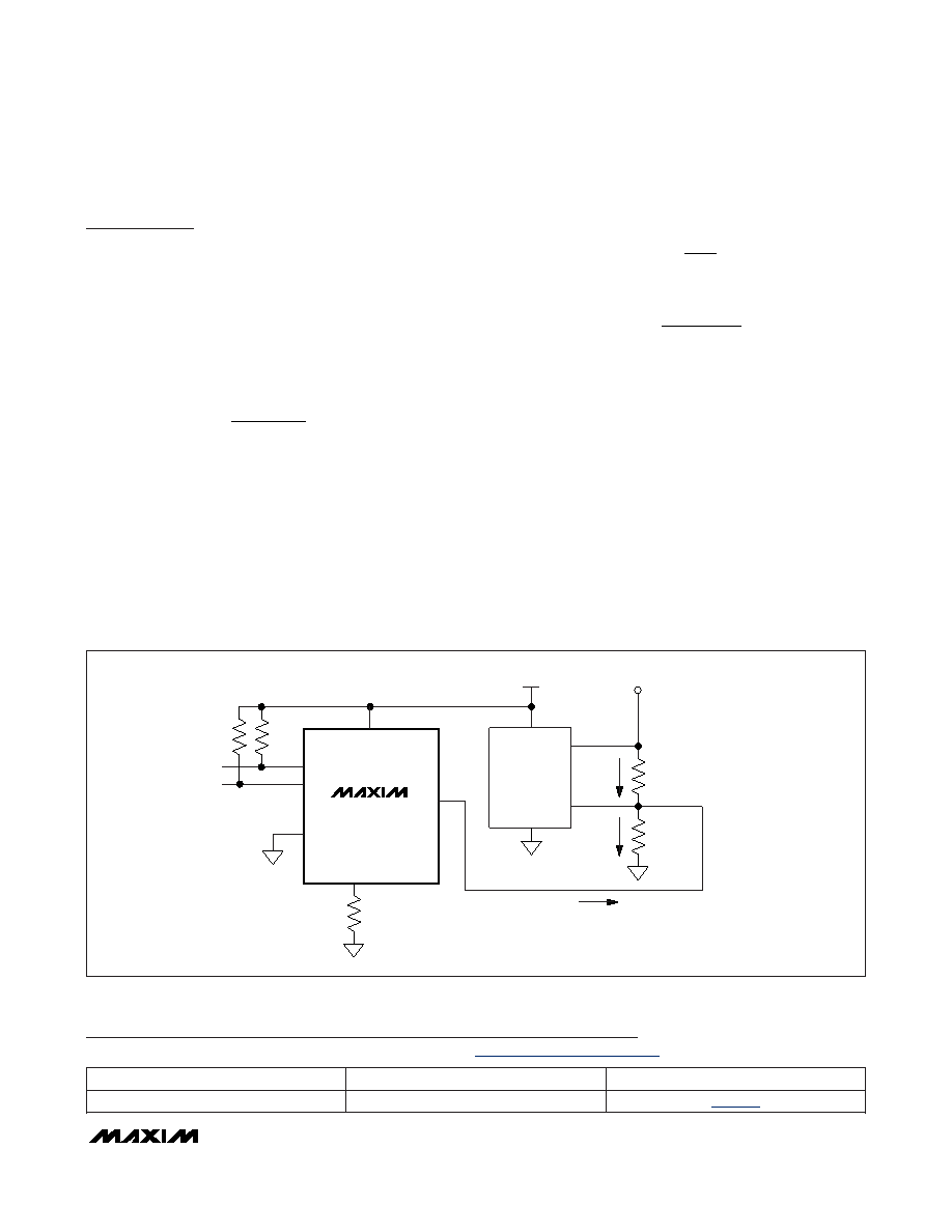
Applications Information
Example Calculation
for an Adjustable Power Supply
In this example, the Typical Operating Circuit is used
as a base to create Figure 3, a 2.0V voltage supply with
±20% margin. The adjustable power supply has a
DC-DC converter output voltage, VOUT, of 2.0V and a
DC-DC converter feedback voltage, VFB, of 0.8V. To
determine the relationship of R0A and R0B, we start with
the equation:
Substituting VFB = 0.8V and VOUT = 2.0V, the relation-
ship between R0A and R0B is determined to be:
R0A = 1.5 x R0B
IOUT0 is chosen to be 1mA (midrange source/sink cur-
rent for the DS4412). Summing the currents into the
feedback node, we have the following
Where:
And
To create a 20% margin in the supply voltage, the value
of VOUT is set to 2.4V. With these values in place, R0B is
calculated to be 267
Ω, and R0A is calculated to be 400Ω.
The current DAC in this configuration allows the output
voltage to be moved linearly from 1.6V to 2.4V using 15
settings. This corresponds to a resolution of 25.8mV/step.
VCC Decoupling
To achieve the best results when using the DS4412,
decouple the power supply with a 0.01F or 0.1F
capacitor. Use a high-quality ceramic surface-mount
capacitor if possible. Surface-mount components mini-
mize lead inductance, which improves performance,
and ceramic capacitors tend to have adequate high-
frequency response for decoupling applications.
I
VV
R
RA
OUT
FB
A
0
=
I
V
R
RB
FB
B
0
=
II
I
OUT
R B
R A
00
0
=
V
R
RR
V
FB
B
AB
OUT
=
+
×
0
00
DC-DC
CONVERTER
FB
OUT
SDA
SCL
OUT0
GND
RFS0 = 4.612k
Ω
4.7k
Ω
4.7k
Ω
VCC
VOUT = 2.0V
FS0
R0B = 267
Ω
R0A = 400
Ω
VFB = 0.8V
IR0A
IR0B
IOUT0
DS4412
Figure 3. Example Application Circuit
PACKAGE TYPE
PACKAGE CODE
DOCUMENT NO.
8 SOP
U8+1
Package Information
For the latest package outline information and land patterns, go to www.maxim-ic.com/packages.
发布紧急采购,3分钟左右您将得到回复。
相关PDF资料
DS4424N+
IC DAC 7BIT 4CH 5.5V 14-TDFN
DS4425BN+
IC OSC CLOCK 425MHZ 10-LCCC
DS4426T+T&R
IC DAC I2C-MARGINING 4CH 28-TQFN
DS4432U+
IC DAC 7BIT 2CH 5.5V 8-MSOP
DS4625P+150/200
IC OSC CLOCK 200MHZ 10-LCCC
DS4M133D+33
IC OSC CLOCK 133.33MHZ 10-LCCC
DS8005-RRX+
SMART CARD AFE DUAL 28SOIC
DSD1792DB
IC 24BIT STEREO AUD DAC 28-SSOP
相关代理商/技术参数
DS4412U+T&R
制造商:Maxim Integrated Products 功能描述:DAC 2CH 4BIT 8USOP - Tape and Reel 制造商:Maxim Integrated Products 功能描述:IC DAC DUAL CH I2C ADJ 8-USOP
DS4412U+T&R
功能描述:数模转换器- DAC 2 Ch I2C Adj Sink/Source Current RoHS:否 制造商:Texas Instruments 转换器数量:1 DAC 输出端数量:1 转换速率:2 MSPs 分辨率:16 bit 接口类型:QSPI, SPI, Serial (3-Wire, Microwire) 稳定时间:1 us 最大工作温度:+ 85 C 安装风格:SMD/SMT 封装 / 箱体:SOIC-14 封装:Tube
DS4412U+TR
制造商:MAXIM 制造商全称:Maxim Integrated Products 功能描述:Dual-Channel, I2C Adjustable Sink/Source Current DAC
DS4412UR
制造商:MAXIM 制造商全称:Maxim Integrated Products 功能描述:Dual-Channel, I2C Adjustable Sink/Source Current DAC
DS4412UT
制造商:MAXIM 制造商全称:Maxim Integrated Products 功能描述:Dual-Channel, I2C Adjustable Sink/Source Current DAC
DS441405-BA
功能描述:CAP FILM 4UF 440VAC QC TERM RoHS:是 类别:电容器 >> 薄膜 系列:PMF 特色产品:ECW-H(C) Series Film Capacitors 标准包装:100 系列:ECW-H(C) 电容:0.33µF 额定电压 - AC:- 额定电压 - DC:630V 电介质材料:聚丙烯,金属化 容差:±3% ESR(等效串联电阻):- 工作温度:-40°C ~ 105°C 安装类型:通孔 封装/外壳:径向 尺寸/尺寸:0.815" L x 0.579" W(20.70mm x 14.70mm) 高度 - 座高(最大):1.028"(26.10mm) 端子:PC 引脚 引线间隔:0.394"(10.00mm) 特点:高频和高稳定性 应用:- 包装:散装 其它名称:ECWH6334HCBP15432
DS4414FP00K
制造商:Thomas & Betts 功能描述:400A,CON,3P4W,MG,414,3P600V,CC
DS4414FR000
制造商:Thomas & Betts 功能描述:400A,REC,3P4W,MG,414,3P600V